A short introduction to CIGS technology
What does CIGS mean?
CIGS thin-film technology is one of the most powerful and long-term stable thin-film processes.
The main component of photovoltaic modules using CIGS technology is a semiconductor layer approximately two micrometers thick. The abbreviation CIGS stands for the components copper (C), indium (I), gallium (G) and selenium (Se) from which this layer is made. AVANCIS combines the four basic elements with sulphur (S) for its special CIGS thin-film technology.

What does CIGS look like under the microscope?
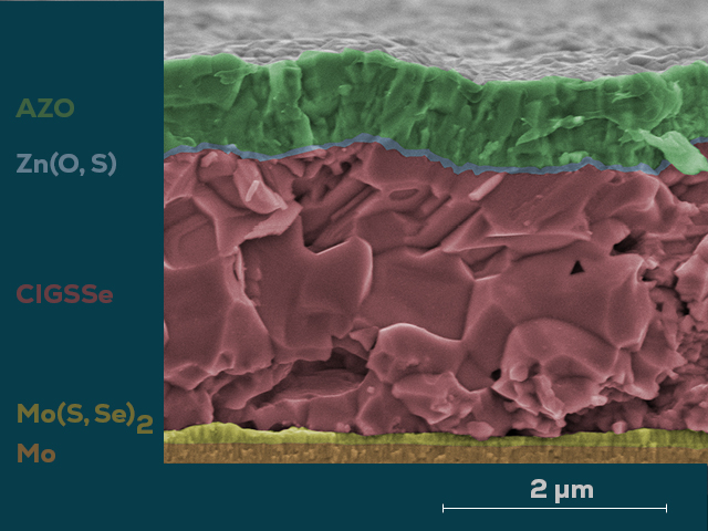
The above image shows a microscopic cross-section of the layer structure of the cadmium/Cd-free AVANCIS CIGS thin-film technology, taken with the aid of a scanning electron microscope (SEM).
Starting with the bottom layer, the molybdenum/Mo back-contact layer, which is deposited on the substrate glass, can be seen in orange.
This layer is followed by a molybdenum sulphoselenide layer/Mo(S, Se)2 - colored yellow, which is formed in the AVANCIS sulphoselenization process by the reaction of sulphur and selenium with the Mo back contact. The Mo(S,Se)2 layer ensures a very good, barrier-free electrical connection between the overlying layer and the Mo back contact.
This overlying positively conducting CIGSSe layer - colored red - is the absorber layer.
A thin so-called buffer layer is then deposited on the CIGS absorber layer, which in the case of AVANCIS CIGS technology consists of Cd-free zinc oxide sulphide/Zn(O,S) - colored blue.
The layer stack is completed by a negatively conducting aluminum-doped zinc oxide layer/AZO - colored green.
How CIGS is manufactured?
These thin layers are produced in various process steps in a vacuum. Our solar factory in Torgau consists of a large number of highly automated vacuum coating systems as well as transport, preparation and post-processing machines. During the coating process, the respective material is atomized under vacuum and applied to the glass under the influence of directed magnetic fields, which is finalized into a solar module after completion of the entire coating process.
By specifically adjusting the mixing ratio of the five components Cu, In, Ga, Se and S during the coating process, the subsequent conversion of sunlight into electrical energy can be specifically influenced and optimized.
This advantageous property of CIGS technology is used, among other things, to optimize the efficiency of the modules even with low solar irradiation and to minimize the influence of increased temperatures on the module output. This ensures maximum annual energy yield.